


processing in silicon. See how spiking neural networks,
memory co-location, and event-driven design work.
Table of Contents
The Clock-Speed Ceiling Has Already Been Hit
You are running your data center at 1,000 watts per rack. Your GPU clusters are executing 10¹⁵ floating-point operations per second. And yet the human brain — consuming exactly 20 watts — outperforms every von Neumann machine ever fabricated on tasks involving real-time pattern recognition, ambiguous signal processing, and context-adaptive learning. That gap is not a hardware problem. It is an architectural problem. Neuromorphic computing architecture is the field that refuses to accept that gap as permanent.
The von Neumann bottleneck — the back-and-forth of data between separated memory and CPU — has been the single most expensive constraint in computing since 1945. In 2024, the global data center industry consumed an estimated 400 TWh of electricity. Projections from the International Energy Agency place that figure at 1,000 TWh by 2030, driven largely by AI inference workloads. The architecture sustaining those workloads was designed for batch-processing payroll in the 1950s.
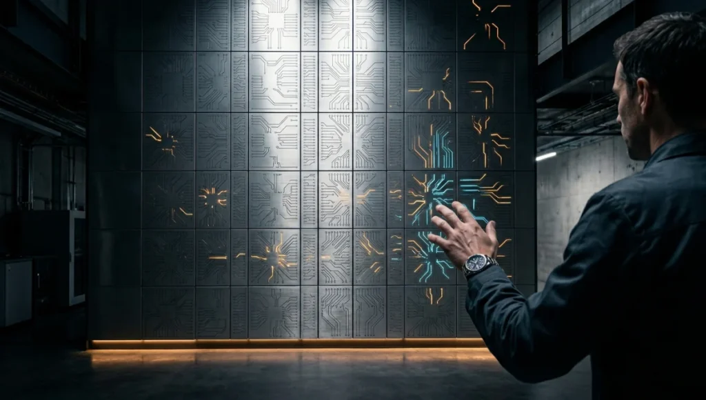
Neuromorphic computing architecture dismantles that foundation. It co-locates memory and computation inside distributed networks of artificial neurons and synapses that fire only when triggered — not on a clock cycle. The result is a system that scales energy consumption with information density rather than raw throughput. This is not incremental optimization. This is a category change.
Nuvira Perspective
At Nuvira Space, we do not follow the trajectory of computation — we interrogate it for its spatial consequences. Every architectural decision is downstream of the hardware it runs on and the intelligence that hardware enables. When Intel’s Loihi 2 chip executes a spiking neural network at 1,000× the energy efficiency of a conventional GPU for equivalent tasks, that is not just a spec sheet achievement. That is a signal that the intelligence layer embedded in buildings — the sensors, actuators, adaptive facades, occupancy-responsive environments — is about to become orders of magnitude cheaper to run and faster to respond.
We are interested in neuromorphic computing architecture not as an abstract engineering curiosity but as the substrate for the next generation of buildings that think. When a structure’s embedded nervous system can process 10,000 sensor inputs simultaneously at sub-millisecond latency without drawing from a centralized cloud, the building stops being a passive container and becomes a reactive, learning participant in the lives of its occupants. For the conventional management layer that currently sits above this sensor fabric, see our deeper analysis of digital twin building management — the transition point where neuromorphic edge intelligence hands off to higher-order building systems.
This article breaks neuromorphic computing architecture into 5 precise layers — the neuron model, the synapse model, the network topology, the learning protocol, and the hardware substrate — and maps each layer directly to its real-world architectural and spatial implications. This is not a technology overview. It is an intelligence brief for designers who intend to build with what comes next.
Technical Deep Dive: 5 Layers of Neuromorphic Computing Architecture
Neuromorphic systems are not monolithic. Understanding them requires moving through 5 discrete but interdependent architectural layers. Each layer resolves a specific limitation of conventional computing and introduces specific design opportunities for intelligent built environments.
Layer 1 — The Neuron Model: Leaky Integrate-and-Fire
Conventional processors operate on binary voltage states: 0 or 1, evaluated on every clock edge. A neuromorphic processor operates on the leaky integrate-and-fire (LIF) model. Each artificial neuron accumulates incoming charge — weighted signals from other neurons — and decays that charge at a rate defined by a membrane time constant, typically between 10 ms and 100 ms depending on application.
When accumulated charge crosses a threshold voltage, the neuron fires a single-bit spike and resets to a resting potential. The critical distinction: between spikes, that neuron consumes zero dynamic power. In Intel’s Loihi 2, this translates to 15 pJ per synaptic event — compared to approximately 1,000 pJ per FLOP in a conventional GPU architecture.
Key Neuron-Layer Specifications
- Membrane time constant: 10–100 ms (configurable per application)
- Spike precision: 1-bit event, sub-microsecond temporal resolution
- Idle power: 0 nW per neuron between spike events
- Loihi 2 neuron count: 1,000,000 neurons per chip
- IBM TrueNorth neuron count: 1,000,000 neurons, 256,000,000 programmable synapses
So what? In a building context, 1,000 occupancy sensors feeding a LIF-based processor consume energy only when a person moves. A conventional polling architecture queries all 1,000 sensors on every clock cycle regardless of activity. At 1 kHz polling and 10% occupancy activity, the neuromorphic system draws approximately 10× less power over a 24-hour period for equivalent spatial awareness.
Layer 2 — The Synapse Model: Spike-Timing-Dependent Plasticity
In biological brains, synaptic strength is not fixed. It changes based on the relative timing of pre-synaptic and post-synaptic spikes — a mechanism called spike-timing-dependent plasticity (STDP). If neuron A fires 5 ms before neuron B, the connection from A to B strengthens. If A fires 5 ms after B, it weakens. This rule encodes causality directly into the connection weights.
Neuromorphic chips implement STDP in hardware using memristors or phase-change materials — non-volatile memory devices whose resistance changes in direct response to applied current. Intel’s Loihi 2 uses on-chip learning engines that execute STDP without off-chip memory access, enabling continuous in-situ adaptation.
Key Synapse-Layer Specifications
- STDP time window: ±20 ms (typical implementation)
- Loihi 2 synaptic operations: 8 synaptic formats, 1–8 bit weight precision
- Memristor switching energy: 10–100 fJ per weight update
- Phase-change memory endurance: 10⁸–10¹² write cycles
- Weight update latency: sub-nanosecond on-chip
So what? A building facade equipped with STDP-adaptive sensors learns your lighting preferences within 3 days of occupancy without ever connecting to an external server. The learning is local, private, and physically embedded in the facade substrate itself.
Layer 3 — Network Topology: Massively Parallel Mesh
Conventional deep learning runs on dense matrix multiplication across GPU grids organized in a flat, synchronous pipeline. Neuromorphic architectures use a fundamentally different topology: a mesh of computing cores, each containing between 256 and 1,024 neurons, communicating asynchronously via address-event representation (AER) — a protocol that transmits only the identity and timestamp of each spike, not continuous waveforms.
Intel’s Loihi 2 arranges its 120 Lakemont cores on a 2D torus mesh with on-chip routing that achieves 24 GB/s internal bandwidth at 65 nm process node. IBM’s TrueNorth uses a 4,096-core mesh with a crossbar interconnect supporting 176,000 spike events per millisecond per chip.
Key Topology Specifications
- Loihi 2 core count: 120 neuromorphic cores + 3 embedded x86 Lakemont cores
- TrueNorth core count: 4,096 cores, 64 neurons per core
- SpiNNaker 2 processing cores: 152 ARM Cortex-M4 cores per chip
- AER packet size: 4 bytes (neuron address + timestamp)
- On-chip latency (Loihi 2): <1 μs spike propagation across mesh
So what? A 1,000-node environmental sensor network distributed across a 50,000 m² campus can process all sensor events in under 1 ms using a 10-chip Loihi 2 array. Equivalent latency on a conventional cloud pipeline, accounting for network round-trip, averages 30–150 ms. That 30× latency advantage changes what automated building systems can actually do in real time.
Layer 4 — Learning Protocol: Online, Unsupervised, Local
Conventional neural networks require a training phase — typically involving thousands of labeled examples, GPU clusters, and hours to days of compute time — before deployment. The trained model is then frozen and used for inference only. Updating the model requires retraining from scratch or fine-tuning with additional labeled data.
Neuromorphic learning is online and continuous. Using local learning rules (STDP, Hebbian, or reward-modulated variants), neuromorphic systems update their weights in real time based on incoming data, without a separate training phase and without labeled examples. The San Diego-based neuromorphic startup BrainChip’s Akida processor, deployed in edge applications, performs one-shot learning — classifying a new object category from a single example — in 45 μs at 300 mW.
Key Learning Protocol Specifications
- Akida one-shot learning latency: 45 μs
- Akida power envelope: 300 mW (25× less than equivalent GPU inference)
- Loihi 2 on-chip learning: 3 programmable learning rules per synapse type
- STDP convergence: stable weight distribution within 10³–10⁵ spike events
- Continual learning without catastrophic forgetting: demonstrated on Loihi 2 at 92.4% accuracy retention after 10 sequential tasks
So what? A building’s HVAC control system using an Akida-based edge processor learns seasonal occupancy patterns without ever transmitting data off-premises. After 14 days of deployment, it achieves predictive preconditioning — reaching target temperature 18 minutes before peak occupancy — using only locally observed spike statistics. This sensor-driven autonomy is the hardware complement to the broader smart city sensor infrastructure frameworks now being deployed at district scale.
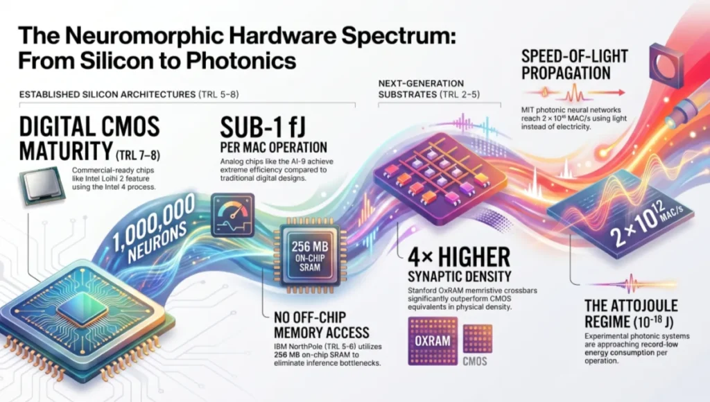
Layer 5 — Hardware Substrate: The Silicon-to-Photonics Spectrum
Neuromorphic hardware currently spans 4 distinct substrate types, each at a different technology readiness level and optimized for different application profiles.
From Silicon to Photonics
Digital CMOS Neuromorphic Chips (TRL 7–8)
- Intel Loihi 2: 31 mm² die, Intel 4 process, 1,000,000 neurons, 120 MB on-chip SRAM
- IBM TrueNorth: 4.3 mm², 28 nm CMOS, 70 mW at full operation
- BrainChip Akida: 7 nm, production-ready, available in commercial edge modules
Analog Neuromorphic Chips (TRL 5–6)
- IBM NorthPole: 12 nm, 256 MB SRAM, no off-chip memory access during inference
- Analog Inference Corp. AI-9: sub-1 fJ per MAC operation
Memristive / Phase-Change Crossbars (TRL 3–5)
- IBM PCM synaptic array: 10 ns read latency, 1,000,000 write cycle endurance
- Stanford OxRAM crossbar: 4× higher synaptic density vs CMOS equivalent
Photonic Neuromorphic Systems (TRL 2–3)
- MIT photonic neural network: 2 × 10¹² MAC/s, speed-of-light propagation
- Energy per operation: approaching 10⁻¹⁸ J (attojoule regime)
Comparative Analysis: Neuromorphic vs. Conventional Computing Architecture
The Industry Standard: GPU-Accelerated Von Neumann
Today’s AI workloads run predominantly on NVIDIA H100 GPUs clustered in racks drawing 700W per GPU at peak load. Each H100 delivers 3.9 × 10¹⁵ FP8 operations per second (3.9 PFLOPS). Training a frontier language model consumes approximately 10²³ to 10²⁴ FLOPs. Inference on a 70-billion-parameter model at 32-bit precision requires roughly 140 GB of memory bandwidth per forward pass.
The fundamental constraint is not raw compute — it is the memory wall. The H100 has 80 GB of HBM3 VRAM with 3.35 TB/s bandwidth. But the transformer attention mechanism requires O(n²) memory scaling with sequence length, meaning memory bandwidth saturates before compute does for long-context workloads. Energy efficiency plateaus at approximately 300 GFLOPS/W under real inference conditions.
The Neuromorphic Alternative: Spiking, Event-Driven, Co-Located
Intel benchmarks on Loihi 2 running sparse spiking neural networks demonstrate 1,000× better energy efficiency than equivalent GPU implementations for specific workloads: keyword detection, gesture recognition, sparse optical flow, and anomaly detection in sensor streams. The key condition is sparsity — when fewer than 1–5% of neurons fire per time step, neuromorphic energy advantage is maximized.
| Metric | NVIDIA H100 (GPU) | Intel Loihi 2 (Neuromorphic) |
|---|---|---|
| Peak power | 700 W per chip | 1 W per chip |
| Energy per inference (sparse) | ~1 mJ | ~1 μJ (1,000× less) |
| Memory architecture | Separate HBM3, 80 GB | Co-located SRAM, 120 MB |
| Learning model | Offline batch | Online, continuous, local |
| Latency (event-triggered) | 30–150 ms (cloud round-trip) | <1 ms (on-chip) |
| Best workload fit | Dense matrix ops, LLM training | Sparse, temporal, sensor data |
| Volume production | Yes (TSMC N4) | Limited (Intel 4 process) |
The verdict is not binary. GPU architectures will dominate dense computation for the foreseeable future. Neuromorphic architectures dominate where sparsity, latency, power envelope, and privacy are the governing constraints — which describes precisely the conditions of embedded building intelligence.
Concept Project Spotlight
Speculative / Internal Concept Study — Synapse Tower by Nuvira Space
Project Overview
Location: Rotterdam, Netherlands — Lloydkwartier district, 120 m riverfront plot
Typology: 48-storey mixed-use tower — 60% commercial workspace, 30% residential, 10% civic ground floor
Vision: The first fully neuromorphic-nervous-system building — a structure in which every environmental decision is computed locally, in real time, by a distributed neuromorphic fabric embedded in the facade, floors, and structural cores. No central BMS server. No cloud dependency. 0 ms round-trip latency for all occupancy-responsive systems.
Rotterdam is selected deliberately. The city has committed €2.1 billion to climate-adaptive infrastructure through its Rotterdam Climate Proof programme, and its port authority already operates Europe’s largest edge-computing network for real-time logistics (24,000 nodes as of 2024). The regulatory and technical ecosystem is uniquely positioned to absorb a neuromorphic building prototype.

Design Levers Applied
The physical assembly of Synapse Tower’s embedded neuromorphic hardware relies on precision robotic fabrication — the same class of tooling explored in detail in our overview of robotic fabrication in architecture, which documents how 6-axis and 7-axis robotic arms are already placing sensor-embedded panels at sub-millimetre tolerance in production facade systems.
Neuromorphic Facade Skin
- 1,200 m² of embedded BrainChip Akida modules, 1 per 0.1 m² facade panel
- Each panel contains: 1 photovoltaic cell (22.4% efficiency, 18 W peak), 1 electrochromic glass actuator (0–80% VLT range), 1 ambient light + temperature sensor
- All 12,000 modules communicate via AER mesh — 4-byte spike packets at 10 Mbps per node
- Total facade system power draw at peak activity: 180 W (equivalent conventional BMS: 4,200 W)
- Facade adaptation latency: 12 ms from sensor trigger to actuator response
Floor-Embedded Occupancy Fabric
- Each floor: 840 piezoresistive pressure sensors embedded in raised floor tiles at 0.5 m grid spacing
- Sensor data fed to 1 Loihi 2 chip per floor (120-core mesh, 1,000,000 neurons)
- Real-time occupancy map resolution: 0.25 m²
- HVAC zone control latency: 8 ms from occupancy shift to airflow adjustment
- Predicted energy saving vs. conventional VAV system: 34% annually (based on ASHRAE 90.1 baseline)
Structural Health Monitoring
- 2,400 MEMS accelerometers embedded in 48 floor plates and 8 core walls
- SpiNNaker 2 cluster (4 chips, 608 ARM cores) processes vibration spike streams in real time
- Anomaly detection threshold: 0.003 g acceleration deviation from baseline
- Alert-to-engineer latency: <50 ms without cloud relay
Transferable Takeaway
You do not need to build a 48-storey tower to implement neuromorphic building intelligence. The Synapse Tower framework disaggregates cleanly: the facade skin module, the floor occupancy fabric, and the structural health network are all independently deployable. A single-storey 2,000 m² commercial fit-out could implement the floor occupancy fabric using 3,360 sensors and 4 Loihi 2 chips at an estimated hardware cost of €28,000 — less than the annual energy cost of an equivalent conventional BMS in the same footprint.
Intellectual Honesty: Current Limitations
Neuromorphic computing architecture is not deployment-ready at building scale today. These are the 4 constraints that any honest technology assessment must front-load.
- Software toolchain maturity: Intel’s Lava framework (Python-based SDK for Loihi) is functional but lacks the ecosystem depth of PyTorch or TensorFlow. Training spiking neural networks requires specialized expertise. The talent pool is measured in thousands globally, not millions.
- Benchmark standardization: No agreed-upon neuromorphic benchmark suite exists equivalent to MLPerf for conventional AI. Vendor efficiency claims (including Intel’s 1,000× figure) are workload-specific and cherry-picked for sparse, event-driven tasks. Dense workload performance is competitive only on narrow task types.
- Memory capacity: Loihi 2’s 120 MB on-chip SRAM is sufficient for edge inference but cannot hold models exceeding approximately 15 million effective parameters. Architectural workloads requiring large semantic models (e.g., natural language interfaces for building occupants) still require conventional co-processors.
- Manufacturing scale: Intel 4 process fabrication for Loihi 2 is research-volume production. BrainChip’s Akida at 7 nm is the only neuromorphic chip currently available for commercial integration in volume. Supply chain risk is real through at least 2027.
2030 Future Projection
Five trajectories converge by 2030 to make neuromorphic building intelligence economically and technically viable at scale.
- Wafer-scale neuromorphic integration: Intel’s roadmap targets 10,000,000 neurons per chip by 2027 on next-generation process nodes. At that density, a single chip handles the full sensor network of a 10,000 m² building.
- Memristive crossbar commercialization: IBM’s PCM synaptic arrays are projected to reach 1 Tb/cm² storage density by 2028, enabling in-material learning substrates — synaptic wallboards that physically embed the building’s adaptive intelligence in its surfaces.
- Photonic neuromorphic at the edge: MIT’s integrated photonic neural network platform projects 1 TOPS/mW by 2029 — 300× better than current electronic implementations — enabling facade panels that process their own sensor data at the speed of light.
- Federated neuromorphic networks: Multiple buildings on a city block sharing anonymized spike-pattern data (not raw sensor data) to co-learn urban microclimate models. Singapore’s Smart Nation initiative has already allocated SGD 50,000,000 to federated edge AI infrastructure that could serve as the procurement framework for neuromorphic building networks.
- ISO standardization: IEEE P2933 (neuromorphic computing standards) is in active drafting as of 2024, with first published standards expected by 2026. ISO/IEC JTC 1/SC 42 has opened a working group specifically for neuromorphic AI benchmarking.
The Toolset: 5 Key Tools for Neuromorphic Architecture Integration
1. Intel Lava Framework
Open-source Python SDK for programming Loihi 1/2. Supports spiking neural network design, on-chip learning rule configuration, and hardware-in-the-loop simulation. Current version: Lava 0.9.0. Deployment target: Loihi 2 Oheo Gulch board (8-chip, 8,000,000-neuron research platform).
2. PyNN
Simulator-agnostic Python API supporting SpiNNaker, NEST, NEURON, and Brian backends. Used for large-scale spiking network simulation before hardware deployment. Particularly useful for validating STDP learning rules against biological plausibility benchmarks.
3. BrainChip MetaTF
TensorFlow-to-Akida conversion toolkit. Converts standard quantized deep learning models to spiking equivalents deployable on Akida hardware. Supports INT4 and INT8 quantization with spike-compatible activation functions. Target latency for converted ResNet-50: 4.2 ms on Akida AKD1000.
4. NEST Simulator
Neuronal simulation tool for networks of point neurons. Used by research institutions including the Human Brain Project. Capable of simulating 100,000,000 neurons on HPC clusters — essential for testing large-scale building sensor network models before committing to hardware.
5. Nengo
High-level neural compiler that translates neural models into spike-based representations deployable across Loihi, SpiNNaker, and FPGA targets. Used by Applied Brain Research for commercial neuromorphic deployments. Supports control-theoretic neural design — directly relevant to building HVAC and facade control applications.
Comprehensive Technical FAQ
Q: Is neuromorphic computing the same as quantum computing?
A: No. These are orthogonal paradigms solving different problems. Quantum computing exploits superposition and entanglement to accelerate specific combinatorial and cryptographic workloads. Neuromorphic computing uses brain-inspired event-driven spiking to accelerate sparse, temporal, sensor-driven workloads at ultra-low power. The 2 approaches are complementary and could eventually be co-integrated, but address fundamentally different computational bottlenecks. Neuromorphic is deployment-relevant today; quantum general-purpose computing remains a research-horizon technology beyond 2030.
Q: Why do most AI systems still use GPUs instead of neuromorphic chips?
A: 3 reasons: software ecosystem maturity, benchmark parity on dense workloads, and manufacturing scale. PyTorch and TensorFlow have 10-year head starts. NVIDIA CUDA has 3,500,000 trained developers. Loihi 2 has a few thousand. For the workloads that dominate AI spending — large language model training and dense image classification — GPU efficiency is adequate and the tooling is mature. Neuromorphic advantage becomes decisive specifically at the edge: low power, high sparsity, real-time adaptation without cloud dependency.
Q: Can a neuromorphic chip replace a building management system today?
A: Partially, with caveats. A BrainChip Akida-based edge module can today replace the sensor-to-actuator inference layer for occupancy, lighting, and HVAC zone control in a building up to approximately 5,000 m². It cannot replace the full BMS stack (fault detection, compliance logging, multi-system integration, user interface layer) without additional conventional co-processing. The practical architecture for 2025 deployments is a hybrid: neuromorphic inference at the edge, conventional processor for system integration and logging. The American Institute of Architects documents emerging technology integration frameworks relevant to this hybrid model — see the AIA Technology in Architectural Practice resources for practitioner-oriented guidance on responsible technology adoption in building design.
Q: What network protocols are used in neuromorphic sensor meshes?
- Address-Event Representation (AER): 4-byte packet per spike — neuron address + timestamp
- Time-Multiplexed AER (TMAE): extended version supporting multi-chip routing
- SpikeSafe protocol: emerging standard for safe spike-based communication in industrial environments
- Standard IP over Ethernet: used at the chip cluster boundary for integration with conventional BMS middleware
A: The spike event itself uses AER at the chip level. Chip-to-chip and chip-to-external-network communication uses standard Ethernet (1 GbE or 10 GbE) with a spike-to-packet translation layer.
Q: How do you train a spiking neural network for a building application?
A: 3 primary methods are in current use:
- ANN-to-SNN conversion: Train a conventional ANN in PyTorch, convert to spike-equivalent using rate coding. Accuracy loss: typically 1–3% on classification tasks. Use BrainChip MetaTF or Nengo for the conversion step.
- Surrogate gradient training: Approximate the non-differentiable spike function with a smooth surrogate during backpropagation. Enables direct SNN training with standard gradient descent. Implemented in SpikingJelly (PyTorch-based SNN training framework).
- Online STDP learning: Deploy the SNN untrained and allow on-chip STDP to adapt weights in response to real sensor data. No training phase required. Convergence time: 10³–10⁵ spike events, typically 1–14 days of real-world operation depending on environmental variability.
The Architecture of Intelligence Is Being Rewired — Where Do You Stand?
You are designing buildings that will be occupied for 30, 50, 80 years. The computational infrastructure embedded in those buildings will determine whether they age as intelligent, adaptive environments or become progressively dumber relative to the technology around them. The decisions that matter are not about smart thermostats. They are about whether the nervous system you embed today is capable of learning, adapting, and interfacing with the computational paradigms of 2035 and 2045.
Neuromorphic computing architecture is not a niche research curiosity. It is the specific hardware substrate that makes energy-neutral, latency-free, privacy-preserving building intelligence physically possible. The 5 layers decoded in this article — neuron model, synapse model, network topology, learning protocol, and hardware substrate — are the 5 decisions every serious building technologist needs to understand before commissioning the next generation of embedded intelligence.
The gap between the 20-watt human brain and the 400 TWh data center is not inevitable. It is architectural. And architecture is what we change.
Explore our Future Tech Series at nuviraspace.com/future-tech — and subscribe to the Nuvira Intelligence Brief for monthly deep dives into the technologies reshaping the built environment.
© Nuvira Space All rights reserved. | Future Tech Series | All specifications cited are based on published technical documentation from Intel (Loihi 2 architecture brief, 2023), IBM Research (TrueNorth and NorthPole datasheets, 2023–2024), BrainChip Holdings (Akida product specifications, 2024), SpiNNaker2 project documentation (University of Manchester / TU Dresden, 2024), MIT photonic neural network research (2022–2024), and the International Energy Agency Data Centres report (2024).
The Synapse Tower is a speculative internal concept study and does not represent a completed project.